Research highlights
The Laboratory of Thin Film and Optics focuses part of R&D activities on the design, fabrication and characterization of multilayer samples using classical thin film materials as well as nanostructured materials with plasmonic behavior. We have a large expertise on the characterization and modeling of materials in thin films using non-destructive optical methods (spectro-photometry and spectroscopic ellipsometry). Once the material properties are known, design of complex multilayer structures is performed using numerical methods. Our latest research activities focus on the fabrication of two and three dimensional photonic microstructures by the electric field assisted dissolution of metal nanoparticles.
Sample preparation
Optical films and multilayer systems are prepared using thin film deposition technique (e-beam evaporation). We are implementing optical monitoring and ion-assisted deposition systems.
Materials
We have a large expertise on the deposition of several materials for optical coating technology: dielectrics (SiO2, TiO2, ZrO2, Y2O3), metals (Ag, Au, Cr) and semiconductors (Si, Ge). Over the last years our research efforts are focused on the study of metal nanoparticles and their surface plasmon resonance (SPR, Figure 1). The SPR leads to strong absorption and scattering of light, with multiple applications in sensing, photovoltaics, medicine and telecommunications. With our fabrication facilities, we produce metal island films , i.e., two-dimensional ensembles of metal nanoparticles deposited on a substrate. By modifying the deposition conditions we can broadly tailor the SPR of metal island films (Figure 2, Reference [1])
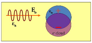
Fig. 1. Surface plasmons in metal nanoparticles
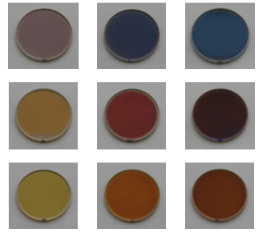
Fig. 2. Metal island films deposited at different conditions
Characterization
Optical characterization of samples is performed using non-destructive methods (spectrophotometry and spectroscopic ellipsometry) in the UV-VIS-NIR range. We also use photothermal deflection spectroscopy in order to determine low absorption levels. The data analysis involves the model development, data fitting and the retrieval of optical constants of materials (Figure 3, Reference [2]). Structural characterization techniques are used to determine the morphological properties of the films, like the size and shape of clusters in metal island films. Results of morphology investigations are correlated with optical measurements.
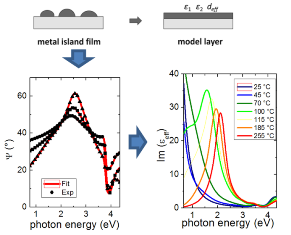
Fig. 3. Spectroscopic ellipsometry analysis: sample model, data fit and optical constants
Numerical simulations
are used to describe the fundamental properties of the surface plasmon resonance, such as the electromagnetic field enhancement (Figure 4). In addition, the effective optical response of composite systems (References [3-5]) is analytically and numerically studied in order to explain the optical behavior of our samples.
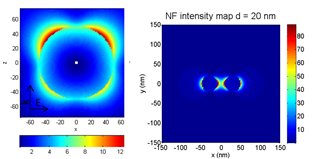
Fig. 4. Numerical simulations: plasmon field enhancement
Design of novel optical multilayers
We have theoretically shown and experimentally proven that multilayer stacks with metal island films (Figure 5) can have significant advantages with respect to classical multilayer coatings for various applications (References [6, 7]).
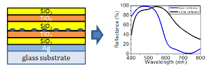
Fig. 5. Optical multilayer systems with metal island films
Photonic structures
are produced using the electric field assisted dissolution of nanoparticles. The application of intense electric field and moderately elevated temperatures allows imprinting two-dimensional patterns on the multilayer structures (Figure 6, Reference [8]). In this way, three-dimensional photonic structures with plasmonic properties can be fabricated (Reference [9]).
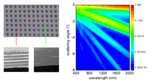
Fig. 6. Three dimensional photonic structures
References
[1] M. Lončarić et al. Vacuum. 84 (2009) , 1; 188-192
[2] M. Lončarić et al. Thin Solid Films. 519 (2011) ; 2946-2950
[3] J. Sancho-Parramon et al. Opt. Express. 18 (2010),26, 26915
[4] J. Sancho-Parramon. Nanotechnology. 20 (2009) , 23; 235706
[5] J. Sancho-Parramon. Journal of Physics D - Applied Physics. 41 (2008) , 21; 215304-1-215304-7
[6] H. Zorc et al. Applied optics 50 (2011) , C364-C367
[7] V. Janicki et al. Applied Optics 50 (2011) C228-C231
[8] J. Sancho-Parramon et al . Applied Physics Letters. 92 (2008) 163108
[9] V. Janicki et al. Applied physics. B, Lasers and optics. 98 (2010) 93-98